US 11,861,280 B2
Device for generating verification vector for circuit design verification, circuit design system, and reinforcement learning method of the device and the circuit design system
In Huh, Seoul (KR); Jeong-hoon Ko, Hwaseong-si (KR); Hyo-jin Choi, Seoul (KR); Seung-ju Kim, Suwon-si (KR); Chang-wook Jeong, Hwaseong-si (KR); Joon-wan Chai, Seoul (KR); Kwang-il Park, Yongin-si (KR); Youn-sik Park, Hwaseong-si (KR); Hyun-sun Park, Seoul (KR); Young-min Oh, Suwon-si (KR); Jun-haeng Lee, Hwaseong-si (KR); and Tae-ho Lee, Suwon-si (KR)
Assigned to SAMSUNG ELECTRONICS CO., LTD., Suwon-si (KR)
Filed by SAMSUNG ELECTRONICS CO., LTD., Suwon-si (KR)
Filed on Mar. 11, 2022, as Appl. No. 17/692,883.
Application 17/692,883 is a division of application No. 16/788,924, filed on Feb. 12, 2020, granted, now 11,281,832.
Claims priority of application No. 10-2019-0016842 (KR), filed on Feb. 13, 2019.
Prior Publication US 2022/0198111 A1, Jun. 23, 2022
Int. Cl. G06F 30/33 (2020.01); G06N 3/08 (2023.01)
CPC G06F 30/33 (2020.01) [G06N 3/08 (2013.01)] 20 Claims
OG exemplary drawing
 
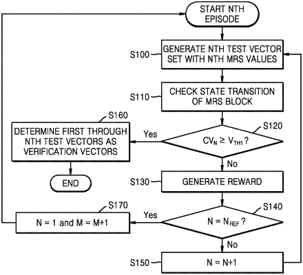
1. A method of reinforcement learning of a neural network device for generating a verification vector for verifying a circuit design comprising a circuit block, the method comprising:
inputting a test vector to the circuit block;
generating at least one reward according to a change in a coverage corresponding to the test vector, the coverage being determined based on a state transition of the circuit block based on the test vector; and
applying the at least one reward to a reinforcement learning.