| CPC G06F 3/0446 (2019.05) [G06F 3/0445 (2019.05); G06F 3/04164 (2019.05)] | 10 Claims |
|
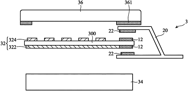
1. A substrate assembly, comprising:
a first substrate comprising an edge;
an active element layer disposed on the first substrate;
a plurality of first electrodes disposed on the first substrate and between the edge and an edge of the active element layer, and arranged along a first direction, wherein at least one of the plurality of first electrodes is electrically connected to the active element layer;
a first register mark disposed on the first substrate;
a circuit substrate partially overlapping the first substrate in a vertical projection direction; and
a plurality of second electrodes disposed on the circuit substrate, and
wherein an offset distance is formed between one of the plurality of second electrodes and one of the plurality of first electrodes in the first direction, and a width of the one of the plurality of first electrodes is different from a width of the one of the plurality of second electrodes.
|