| CPC G06F 3/0443 (2019.05) [G06F 3/0412 (2013.01); G06F 3/0446 (2019.05); G09G 3/3225 (2013.01); H10K 50/8445 (2023.02); H10K 59/40 (2023.02); G06F 2203/04102 (2013.01); G06F 2203/04103 (2013.01); G06F 2203/04111 (2013.01); H10K 59/12 (2023.02)] | 19 Claims |
|
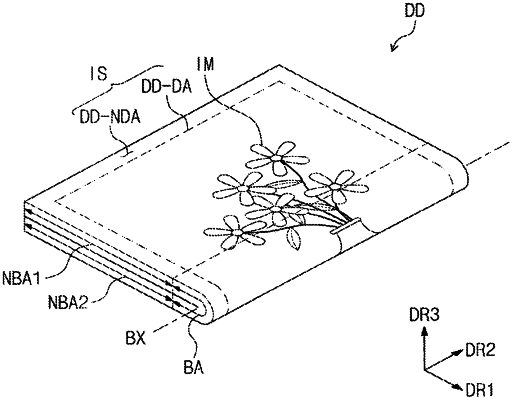
1. A display device comprising:
an organic light emitting device layer;
a thin film encapsulation layer on the organic light emitting device layer, the thin film encapsulation layer having a first surface adjacent to the organic light emitting device layer and a second surface opposite the first surface and spaced from the organic light emitting device layer;
a buffer layer directly on the second surface of the thin film encapsulation layer; and
a touch sensing unit directly on the buffer layer, the touch sensing unit comprising:
a first conductive pattern on the buffer layer;
an insulating layer covering the first conductive pattern; and
a second conductive pattern on the insulating layer and electrically insulated from the first conductive pattern, the second conductive pattern having a thickness above the first conductive pattern in a thickness direction of the display device that is greater than a thickness of the first conductive pattern in the thickness direction of the display device.
|