| CPC G06F 3/0412 (2013.01) [G02F 1/13338 (2013.01); G06F 3/0443 (2019.05); G06F 3/0445 (2019.05); G06F 3/0446 (2019.05); H01L 27/1248 (2013.01); H01L 27/156 (2013.01); H10K 59/122 (2023.02); H10K 59/123 (2023.02); H10K 59/124 (2023.02); H10K 59/1213 (2023.02); H10K 59/40 (2023.02); G06F 2203/04105 (2013.01); G06F 2203/04111 (2013.01)] | 24 Claims |
|
1. A light-emitting diode (“LED”) device, comprising:
a flexible polymer substrate;
a buffer layer on the flexible polymer substrate, substantially totally covering a top surface of the flexible polymer substrate;
a plurality of thin film transistors (“TFT”s) on the buffer layer, each TFT comprising an active layer, a gate electrode, a source electrode, and a drain electrode;
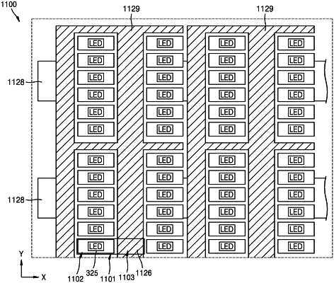
a plurality of LEDs, each electrically connected to one of the plurality of TFTs;
a touch sensor comprising first sensor electrodes and second sensor electrodes on the flexible polymer substrate;
connecting wires on the flexible polymer substrate; and
dummy patterns, which are in a floating state and disposed on the flexible polymer substrate;
wherein a pair of first sensor electrodes are electrically connected to each other via one of the connecting wires,
wherein the touch sensor senses a capacitance change generated between one of the first sensor electrodes and one of the second sensor electrodes,
wherein the first sensor electrodes, the second sensor electrodes, and the dummy patterns are arranged on the same layer,
wherein the touch sensor, the connecting wires, the source electrode, the drain electrode and the dummy patterns comprise metallic materials,
wherein, in a plan view, a first portion of the one of the first sensor electrodes mainly extends in a first direction and a second portion of the one of first sensor electrodes mainly extends in a second direction intersecting the first direction,
wherein, in a plan view, the second portion of the one of the first sensor electrodes is disposed between a pair of LEDs from among the plurality of LEDs immediately next to each other in the first direction and overlaps the first portion of the one of the first sensor electrodes in the second direction, and
wherein, in a plan view, a side of one of the pair of LEDs faces the second portion of the one of the first sensor electrodes and an opposite side of the one of the pair of LEDs opposite to the side of the one of the pair of LEDs in the first direction is exposed to the one of the second sensor electrodes.
|