| CPC G06F 13/1668 (2013.01) [H01L 25/0657 (2013.01); G11C 7/10 (2013.01); G11C 8/10 (2013.01); H01L 2225/06541 (2013.01)] | 19 Claims |
|
1. A memory device comprising:
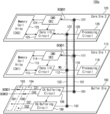
a buffer die configured to receive a first broadcast command from an external device through a first channel, receive a second broadcast command from the external device through a second channel, receive a processing command and external data from the external device, and transmit the first and second broadcast commands, the processing command and the external data through first and second through silicon vias (TSVs); and
first and second core dice stacked on the buffer die and respectively allocated to the first and second channels;
wherein the first core die comprises a first memory cell array, a first command decoder configured to decode the first broadcast command transmitted through the first TSV, and a first data input/output circuit configured to output first data of the first memory cell array to a common data input/output bus under control of the first command decoder,
wherein the second core die comprises a processing circuit, a second memory cell array, a second command decoder configured to decode the second broadcast command transmitted through the first TSV, and a second data input/output circuit configured to receive the first data of the first memory cell array from the common data input/output bus under control of the second command decoder, and
wherein the processing circuit is configured to decode the processing command and generate second data by performing a processing operation on the first data and the external data.
|