| CPC G06F 11/1068 (2013.01) [G06F 11/0772 (2013.01); G06F 11/1048 (2013.01); H03M 13/1108 (2013.01)] | 20 Claims |
|
1. A semiconductor memory device comprising:
a memory cell array;
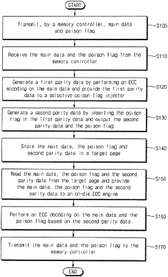
an on-die error correction code (ECC) engine, based on an ECC, configured to, in a write operation:
perform an ECC encoding operation on main data received from a memory controller to generate first parity data;
selectively replace a portion of the first parity data with a poison flag to generate second parity data based on a poison mode signal, wherein the poison mode signal designates a normal mode or a poison mode;
output the second parity data and the poison flag;
provide the main data to a normal cell region in a target page of the memory cell array; and
provide the first parity data to a parity cell region in the target page in the normal mode or provide the poison flag and the second parity data to the parity cell region in the poison mode; and
a control logic circuit configured to control the on-die ECC engine and to generate the poison mode signal based on a command and an address from the memory controller.
|