US 11,860,731 B2
Channel modulation for a memory device
Martin Brox, Munich (DE); Peter Mayer, Neubiberg (DE); Wolfgang Anton Spirkl, Germering (DE); Thomas Hein, Munich (DE); Michael Dieter Richter, Ottobrunn (DE); Timothy M. Hollis, Meridian, ID (US); and Roy E. Greeff, Boise, ID (US)
Filed by Lodestar Licensing Group LLC, Evanston, IL (US)
Filed on Jul. 5, 2022, as Appl. No. 17/857,700.
Application 17/857,700 is a continuation of application No. 16/744,025, filed on Jan. 15, 2020, granted, now 11,409,595.
Claims priority of provisional application 62/793,585, filed on Jan. 17, 2019.
Prior Publication US 2022/0334915 A1, Oct. 20, 2022
This patent is subject to a terminal disclaimer.
Int. Cl. G06F 11/00 (2006.01); G06F 11/10 (2006.01); G06F 11/16 (2006.01); G06F 12/02 (2006.01)
CPC G06F 11/1004 (2013.01) [G06F 11/16 (2013.01); G06F 12/02 (2013.01)] 20 Claims
OG exemplary drawing
 
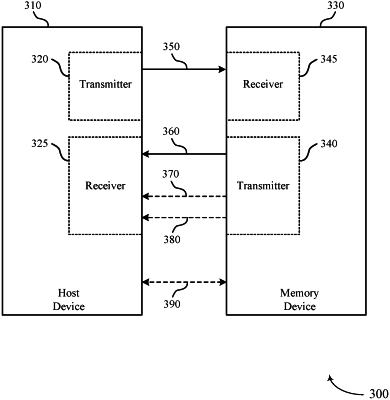
1. A method, comprising:
transmitting first signaling, by a first device over a first channel between the first device and a second device, the first signaling modulated using a first modulation scheme that includes a first quantity of voltage levels spanning a first range of voltages; and
transmitting second signaling, by the first device over a second channel between the first device and the second device, the second signaling modulated using a second modulation scheme that includes a second quantity of voltage levels spanning a second range of voltages smaller than the first range of voltages.