| CPC G06F 1/10 (2013.01) | 19 Claims |
|
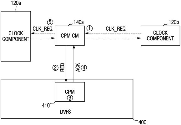
1. A semiconductor device comprising:
a first clock circuit that transmits a first request indicating a processor does not want to receive a clock signal;
a clock manager circuit that transmits a second request indicating the processor does not want to receive the clock signal in response to receiving the first request; and
a dynamic voltage frequency scaling (DVFS) circuit that, in response to receiving the second request, discontinues generating a code applied to regulating a clock frequency at which the processor operates and transmits a first acknowledgment to the clock manager circuit.
|