| CPC G06F 13/1668 (2013.01) [G06F 3/061 (2013.01); G06F 3/065 (2013.01); G06F 3/0683 (2013.01); G06F 13/4022 (2013.01); G06F 13/4282 (2013.01); H03M 13/154 (2013.01); G06F 2213/0026 (2013.01)] | 28 Claims |
|
1. A system, comprising:
a first Non-Volatile Memory Express (NVMe) Solid State Drive (SSD);
a second NVMe SSD;
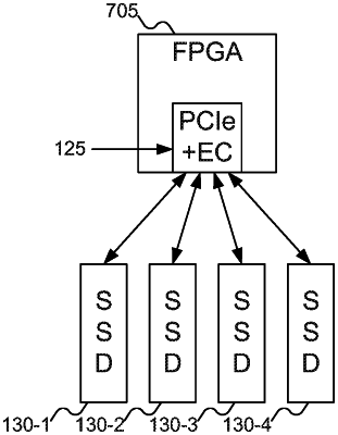
a Field Programmable Gate Array (FPGA), the FPGA implementing one or more functions supporting the first NVMe SSD, the functions comprising at least one of data acceleration, data deduplication, data integrity, data encryption, and data compression, and including a Peripheral Component Interconnect Express (PCIe) switch, the PCIe switch including a processing circuit configured to direct an NVMe storage command, sent to the system, to the FPGA;
wherein the PCIe switch communicates with the FPGA and is connected to the first NVMe SSD, and
wherein the PCIe switch receives the NVMe storage command sent to the system and delivers the NVME storage command to the FPGA based at least in part on the processing circuit.
|