| CPC G05B 19/4099 (2013.01) [G05B 2219/45031 (2013.01); H01L 21/67155 (2013.01); H01L 21/67276 (2013.01)] | 20 Claims |
|
1. A semiconductor manufacturing system, comprising:
at least one semiconductor manufacturing apparatus, comprising:
a series of manufacturing units configured to perform manufacturing operations on wafers;
a first control unit configured to control the manufacturing operations of the series of manufacturing units, and generate log data recording the manufacturing operations of the series of manufacturing units; and
a first storage device cooperatively connected to the first control unit and configured to store the log data transferred from the first control unit; and
a behavior recognition device cooperatively connected to the semiconductor manufacturing apparatus, the behavior recognition device comprising:
a second storage device cooperatively connected to the first control unit of the semiconductor manufacturing apparatus, and configured to store the log data transferred from the first control unit;
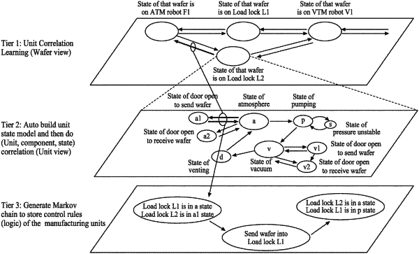
a second control unit cooperatively connected to the second storage device, and configured to receive the log data from the second storage device and build a transition state model to analyze behaviors related to the manufacturing operations of the series of manufacturing units based on the log data; and
a data transmission unit cooperatively connected to the second storage device and the second control unit, and configured to real-time transfer the log data of the semiconductor manufacturing apparatus from the second storage device to the second control unit;
wherein the behavior recognition device is further configured to reproduce an abnormal behavior of the behaviors by performing a simulation based on the transition state model, and adjust a control rule of the manufacturing units according to the reproduced abnormal behavior; and the semiconductor manufacturing apparatus is configured to manufacture a plurality of processed wafers according to the adjusted control rule.
|