| CPC G03F 7/70633 (2013.01) [G03F 7/0035 (2013.01); G03F 7/0043 (2013.01); G03F 7/0047 (2013.01); G03F 7/094 (2013.01); G03F 7/70625 (2013.01); H01L 21/7682 (2013.01); H01L 21/76807 (2013.01); H01L 21/76837 (2013.01); H01L 21/76885 (2013.01); H01L 21/76897 (2013.01); H01L 21/76849 (2013.01)] | 20 Claims |
|
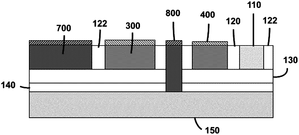
1. A method, comprising:
forming a first sacrificial structure with a first spacer and a second sacrificial structure with a second spacer on a substrate;
forming an opening in a photoresist layer on the first and second sacrificial structures, wherein the opening is above the first and second spacers, and wherein a width of the opening is greater than a width between the first and second spacers;
removing a portion of the substrate between the first and second spacers to form a via opening;
forming a via structure in the via opening;
removing the first sacrificial structure to form a metal line opening;
forming a metal line in the metal line opening; and
forming, on the metal line, a capping layer with a bottom surface coplanar with a top surface of the first spacer.
|