| CPC G02F 1/136286 (2013.01) [G02F 1/1368 (2013.01); G02F 1/136209 (2013.01); G02F 1/136213 (2013.01)] | 10 Claims |
|
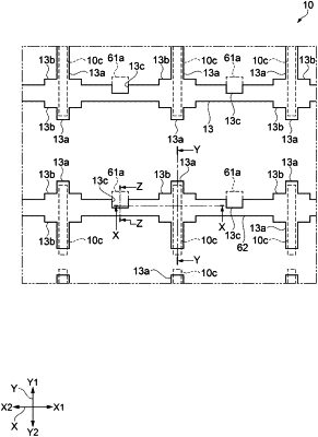
1. An electro-optical device comprising:
a substrate;
a pixel electrode;
a capacitance wiring provided between the substrate and the pixel electrode;
a transistor provided between the substrate and the capacitance wiring;
a light shielding member provided along a first direction between the substrate and the transistor;
a capacitance element provided between the substrate and the light shielding member and overlapping the light shielding member in plan view; and
a conductive member electrically coupled to the capacitance wiring and overlapping the light shielding member in plan view, wherein
the light shielding member includes a cutout portion provided between the conductive member and one electrode of the capacitance element, and
the conductive member and the one electrode of the capacitance element are electrically coupled through a contact hole, at least a portion of the contact hole being provided inside the cutout portion in plan view.
|