| CPC G02F 1/136286 (2013.01) [G02F 1/1337 (2013.01); G02F 1/1362 (2013.01); G02F 1/1368 (2013.01); G02F 1/133345 (2013.01); G02F 1/134363 (2013.01); G02F 1/136277 (2013.01); G09G 3/20 (2013.01); G09G 3/3659 (2013.01); H01L 27/1214 (2013.01); H01L 27/1218 (2013.01); H04N 9/3102 (2013.01); G02F 1/133553 (2013.01); G02F 1/134372 (2021.01); G02F 1/136231 (2021.01); G09G 3/342 (2013.01); G09G 3/3685 (2013.01); G09G 2300/0876 (2013.01); G09G 2310/024 (2013.01); G09G 2310/027 (2013.01); G09G 2310/0235 (2013.01); G09G 2310/0275 (2013.01); G09G 2310/0297 (2013.01); G09G 2320/0233 (2013.01); G09G 2320/0252 (2013.01); G09G 2320/0261 (2013.01); G09G 2320/106 (2013.01); G09G 2340/0435 (2013.01); G09G 2340/16 (2013.01); G09G 2352/00 (2013.01)] | 19 Claims |

|
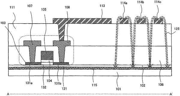
1. A semiconductor device comprising:
a common electrode over a first substrate;
a first conductive layer over the first substrate, the first conductive layer electrically connected to the common electrode;
a semiconductor layer over the first substrate, the semiconductor layer comprising polycrystalline silicon;
a gate wiring, a part of the gate wiring overlapping with the semiconductor layer;
a source wiring, a part of the source wiring being over and in contact with the semiconductor layer;
a second conductive layer over and in contact with the semiconductor layer;
an insulating film over the common electrode, the first conductive layer, and the second conductive layer;
a pixel electrode over the insulating film, the pixel electrode electrically connected to the second conductive layer; and
liquid crystal molecules over the common electrode and the pixel electrode,
wherein the first conductive layer, the source wiring, and the second conductive layer comprise a same material,
wherein the pixel electrode has a plurality of slits,
wherein the part of the gate wiring and a first region of the common electrode overlap with each other, and
wherein the source wiring and a second region of the common electrode overlap with each other.
|