| CPC G02F 1/136286 (2013.01) [G02F 1/136222 (2021.01); H01L 27/1248 (2013.01); G02F 2201/40 (2013.01); G02F 2201/50 (2013.01)] | 20 Claims |
|
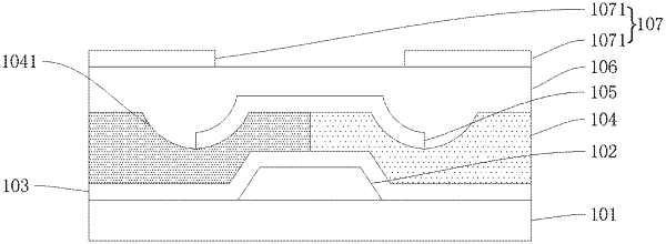
1. A display panel, comprising:
a substrate layer;
a data line arranged on the substrate layer;
a color resist layer disposed on the substrate layer, wherein the color resist layer is located at two sides of the data line and comprises a plurality of grooves, and the plurality of grooves are located at least at one side of the data line;
a shielding layer disposed on the color resist layer and arranged over the data line; and
a pixel electrode layer arranged over the color resist layer and the shielding layer.
|