| CPC G02F 1/13394 (2013.01) [G02F 1/1337 (2013.01); G02F 1/13398 (2021.01); G02F 1/134381 (2021.01); G02F 1/294 (2021.01)] | 9 Claims |
|
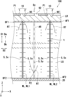
1. A liquid crystal element comprising:
a plurality of unit electrodes each including a first electrode and a second electrode;
a liquid crystal layer to which a voltage is applied from each of the unit electrodes; and
a plurality of wall members arranged in the liquid crystal layer, wherein
the liquid crystal layer has a waveform retardation, and
two or more of a plurality of peaks in the waveform retardation correspond to positions of respective wall members.
|