US 11,860,479 B2
Color conversion panel and display device including the same
Ja Hun Koo, Asan-si (KR); Kyung-Hun Lee, Yongin-si (KR); Tae-Jong Jun, Suwon-si (KR); and Woo-Young Cheon, Suwon-Si (KR)
Assigned to SAMSUNG DISPLAY CO., LTD., Yongin-si (KR)
Filed by SAMSUNG DISPLAY CO., LTD., Yongin-si (KR)
Filed on Dec. 27, 2022, as Appl. No. 18/146,903.
Application 18/146,903 is a continuation of application No. 17/651,162, filed on Feb. 15, 2022, granted, now 11,567,367.
Application 17/651,162 is a continuation of application No. 17/121,207, filed on Dec. 14, 2020, granted, now 11,269,217, issued on Mar. 8, 2022.
Application 17/121,207 is a continuation of application No. 16/541,282, filed on Aug. 15, 2019, granted, now 10,877,318, issued on Dec. 29, 2020.
Application 16/541,282 is a continuation of application No. 15/870,053, filed on Jan. 12, 2018, granted, now 10,409,110, issued on Sep. 10, 2019.
Claims priority of application No. 10-2017-0097724 (KR), filed on Aug. 1, 2017.
Prior Publication US 2023/0142036 A1, May 11, 2023
Int. Cl. G02F 1/1335 (2006.01); G02F 1/13357 (2006.01); G02F 1/1368 (2006.01)
CPC G02F 1/133617 (2013.01) [G02F 1/1368 (2013.01); G02F 1/133504 (2013.01); G02F 1/133509 (2013.01); G02F 1/133514 (2013.01); G02F 1/133526 (2013.01); G02F 1/133528 (2013.01); G02F 1/133614 (2021.01); G02F 1/133621 (2013.01); G02F 2202/36 (2013.01)] 18 Claims
OG exemplary drawing
 
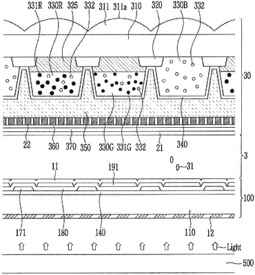
1. A color conversion panel, comprising:
a substrate having a first surface and a second surface opposite to the first surface;
a color conversion portion disposed on the first surface of the substrate, the color conversion portion including a semiconductor nanocrystal;
a light blocking layer disposed between the color conversion portion and the substrate; and
a pattern layer disposed on the second surface,
wherein the pattern layer includes a curved surface,
wherein the color conversion portion at least partially overlaps the pattern layer, and
wherein the light blocking layer overlaps the pattern layer, and
wherein a first side of the light blocking layer facing the color conversion portion and a second side of the light blocking layer facing the substrate have different areas.