| CPC G02F 1/133512 (2013.01) [G02B 26/0858 (2013.01); G02B 26/0875 (2013.01); G02F 1/133514 (2013.01); G09G 3/3648 (2013.01); G09G 3/3674 (2013.01); G09G 2300/0408 (2013.01)] | 20 Claims |
|
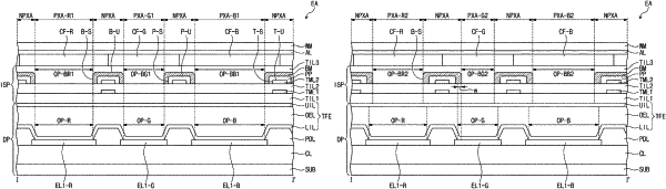
1. A display device comprising:
a display panel including a pixel providing a light; and
an input sensing panel configured to sense an external input, the input sensing panel including:
a first sensing insulating layer disposed on the display panel;
a plurality of first conductive patterns disposed on the first sensing insulating layer;
a second sensing insulating layer disposed on the first sensing insulating layer to cover the first conductive patterns;
a plurality of second conductive patterns disposed on the second sensing insulating layer;
a piezoelectric pattern covering the second conductive patterns;
a light blocking pattern covering the piezoelectric pattern and defining a transmission opening configured to transmit light; and
a third sensing insulating layer disposed on the second sensing insulating layer to cover the light blocking pattern,
wherein the piezoelectric pattern is in direct contact with the second conductive patterns, and
a first voltage is applied to the second conductive patterns in a first mode, and a second voltage different from the first voltage is applied to the second conductive patterns in a second mode.
|
|
11. A display device including:
a display panel including a pixel providing a light; and
an input sensing panel sensing an external input, the input sensing panel including:
a plurality of sensing insulating layers;
a plurality of conductive patterns disposed between the sensing insulating layers;
a piezoelectric pattern covering at least a portion of the conductive patterns; and
a light blocking pattern covering the piezoelectric pattern and defining a transmission opening transmitting the light,
wherein the piezoelectric pattern is in direct contact with the conductive patterns,
a first voltage is applied to the conductive patterns in a first mode, and a second voltage different from the first voltage is applied to the conductive patterns in a second mode, and
the transmission opening has a first width in one direction in the first mode and has a second width smaller than the first width in the one direction in the second mode.
|
|
18. An input sensing panel including:
a first sensing insulating layer;
a plurality of first conductive patterns disposed on the first sensing insulating layer;
a second sensing insulating layer disposed on the first sensing insulating layer to cover the first conductive patterns;
a plurality of second conductive patterns disposed on the second sensing insulating layer;
a piezoelectric pattern covering the second conductive patterns;
a light blocking pattern covering the piezoelectric pattern and defining a transmission opening through which at least a portion of the second sensing insulating layer is exposed; and
a third sensing insulating layer disposed on the second sensing insulating layer to cover the light blocking pattern,
wherein the piezoelectric pattern is in direct contact with the second conductive patterns, and
a first voltage is applied to the second conductive patterns in a first mode, and a second voltage different from the first voltage is applied to the second conductive patterns in a second mode.
|