US 11,860,461 B2
Display panel and method for manufacturing the same
Kai Sui, Beijing (CN); Qian Jin, Beijing (CN); Jinxiang Xue, Beijing (CN); and Wei Huang, Beijing (CN)
Assigned to BOE TECHNOLOGY GROUP CO., LTD., Beijing (CN)
Appl. No. 16/966,697
Filed by BOE TECHNOLOGY GROUP CO., LTD., Beijing (CN)
PCT Filed Oct. 17, 2019, PCT No. PCT/CN2019/111722
§ 371(c)(1), (2) Date Jul. 31, 2020,
PCT Pub. No. WO2021/072707, PCT Pub. Date Apr. 22, 2021.
Prior Publication US 2023/0091595 A1, Mar. 23, 2023
Int. Cl. G02F 1/133 (2006.01); G02F 1/1333 (2006.01); H10K 59/12 (2023.01); H10K 59/122 (2023.01); H10K 59/38 (2023.01); G02F 1/1335 (2006.01)
CPC G02F 1/133354 (2021.01) [H10K 59/1201 (2023.02); H10K 59/122 (2023.02); H10K 59/38 (2023.02); G02F 1/133614 (2021.01); G02F 2201/07 (2013.01)] 20 Claims
OG exemplary drawing
 
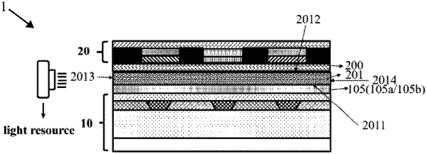
1. A display panel comprising:
a display substrate;
an opposite substrate; and
a first adhesive layer and light guide layer located between the display substrate and the opposite substrate and stacked on each other,
wherein the first adhesive layer comprises a photo-cured layer formed by curing a photocurable material layer, and wherein the light guide layer is used to direct light to the photocurable material layer during the curing to form the photo-cured layer.