| CPC G02B 6/12004 (2013.01) [G02B 6/125 (2013.01); G02B 6/12007 (2013.01); G02B 6/136 (2013.01); G02B 6/29301 (2013.01); G02B 2006/12128 (2013.01)] | 22 Claims |
|
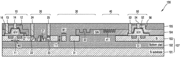
1. A photonic integrated circuit platform comprising:
a substrate;
a first oxide layer disposed on the substrate and comprising an insulating transparent oxide;
a first optical element layer disposed on the first oxide layer and comprising a semiconductor material;
a second optical element layer disposed on the first optical element layer and comprising an insulating material different from the insulating transparent oxide of the first oxide layer, the second optical element layer further comprising a compound semiconductor material different from the semiconductor material of the first optical element layer;
a second oxide layer disposed on the second optical element layer and comprising an insulating transparent oxide; and
a plurality of optical elements formed by patterning the first optical element layer or the second optical element layer,
wherein the plurality of optical elements comprises at least one of a light source or optical amplifier,
wherein the light source or the optical amplifier comprises:
an optical waveguide formed by patterning the semiconductor material of the first optical element layer;
a compound semiconductor layer formed by patterning the compound semiconductor material of the second optical element layer on the optical waveguide;
conductive plugs disposed vertically through the second oxide layer; and
an upper clad disposed to surround an upper portion of the compound semiconductor layer, and
wherein the upper clad comprises the insulating material of the second optical element layer.
|