| CPC G01S 7/032 (2013.01) [H01Q 3/34 (2013.01); H01Q 9/0457 (2013.01)] | 24 Claims |
|
1. A radar arrangement, comprising:
a printed circuit board;
at least one electronic component; and
at least one antenna;
wherein the electronic component is arranged on the printed circuit board and is used at least to generate a high-frequency signal;
at least one line structure, being part of the printed circuit board, for guiding the high-frequency signal from the electronic component into the region of the antenna;
wherein the line structure radiates the high-frequency signal at an open-ended radiation region and impinges the antenna with the radiated high-frequency signal;
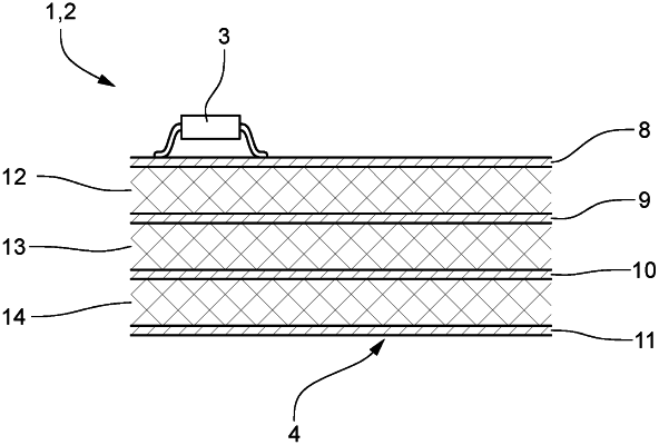
wherein the printed circuit board has at least four electrically conductive layers which run essentially parallel to one another and are separated from one another by at least three electrically insulating layers, so that the first outer layer and the second outer layer are formed by at least two electrically conductive layers of the at least four electrically conductive layers, and the remaining at least two electrically conductive layers form electrically conductive inner layers of the printed circuit board;
wherein the first electrically conductive inner layer is adjacent to the first electrically conductive outer layer and the second electrically conductive inner layer is adjacent to the second electrically conductive outer layer, and the at least three electrically insulating layers all form electrically insulating inner layers of the printed circuit board;
wherein the electronic component is arranged on the first electrically conductive outer layer of the printed circuit board;
wherein the antenna is formed at least partially in the second outer layer of the printed circuit board;
wherein the high-frequency signal generated by the electronic component is transmitted to the antenna, which is formed at least partially in the second electrically conductive outer layer of the printed circuit board, through the region of the electrically conductive inner layers and electrically insulating inner layers of the printed circuit board; and
wherein the at least four electrically conductive layers include an electrically conductive layer that forms the radiation region of the line structure for guiding the high-frequency signal, and an electrically conductive layer that includes a fine aperture for defined passage of the electromagnetic radiation radiated by the radiation region of the line structure, and wherein the electrically conductive layer that includes the fine aperture is between the second electrically conductive outer layer and the electrically conductive layer that forms the radiation region of the line structure.
|