| CPC G01R 31/318555 (2013.01) [G01R 31/31727 (2013.01); G01R 31/318572 (2013.01)] | 20 Claims |
|
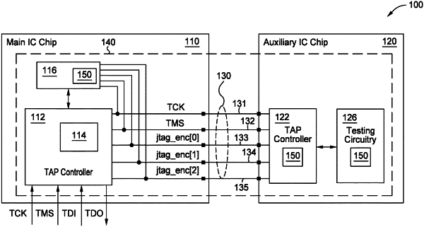
1. An integrated circuit (IC) chip device comprising:
a first IC chip comprising:
first testing circuitry configured to receive a mode select signal, a clock signal, and encoded signals, the first testing circuitry comprising:
finite state machine (FSM) circuitry configured to determine an instruction based on the mode select signal and the clock signal;
decoder circuitry configured to decode the encoded signals to generate a decoded signal; and
control circuitry configured to generate a control signal from the instruction and the decoded signal, wherein the control signal indicates a test to be performed by the first testing circuitry.
|