| CPC G01N 27/20 (2013.01) [H01L 22/34 (2013.01); H01L 23/5228 (2013.01); H01L 28/20 (2013.01)] | 20 Claims |
|
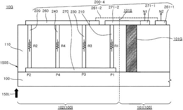
1. A semiconductor device comprising:
a substrate including chip regions and a scribe lane region;
a target layer disposed on the substrate; and
a crack sensor for detecting a crack generated in the target layer,
wherein the crack sensor includes:
a first conductive pattern positioned at a bottom surface of the target layer;
a second conductive pattern positioned on a top surface of the target layer, the top surface being opposite to the bottom surface of the target layer;
a plurality of resistors substantially penetrating the target layer, the plurality of resistors connected in parallel to each other through the first conductive pattern and the second conductive pattern, wherein each of the plurality of resistors is disposed sequentially away from the chip region; and
a first node and a second node connected to the first conductive pattern and the second conductive patterns, respectively.
|
|
17. A semiconductor device comprising:
a target layer disposed on a substrate; and
a crack sensor for detecting a crack generated in the target layer,
wherein the crack sensor includes:
a first conductive pattern positioned at a bottom surface of the target layer;
a second conductive pattern positioned on a top surface of the target layer, the top surface being opposite to the bottom surface of the target layer;
a plurality of resistors substantially penetrating the target layer, the plurality of resistors connected in parallel to each other through the first conductive pattern and the second conductive pattern; and
a first node and a second node connected to the first conductive pattern and the second conductive pattern, respectively.
|