| CPC G01N 21/9501 (2013.01) [G02B 6/122 (2013.01); H01L 21/7624 (2013.01)] | 15 Claims |
|
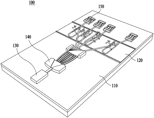
1. A GOI (Ge-on-insulator) device for on-chip optical sensing, the GOI device comprising:
a GOI structure with a waveguide region optical detection element comprising a germanium (Ge) layer;
a light source element configured to generate light for the waveguide region; and
at least one optical detection element configured to detect light coming from the waveguide region,
wherein the optical detection element converts the light from the waveguide region into heat and detects the heat,
wherein the GOI structure comprises:
an insulating substrate; and
a germanium layer integrated on the insulating substrate,
wherein some part of the GOI structure is formed as the waveguide region, and
wherein the optical detection element comprises:
an insulating layer integrated on one side of the waveguide region on the GOI structure and formed to cover the germanium layer on the insulating substrate;
a bolometric material layer stacked on top of the insulating layer, whose resistance changes with heat generated as light is propagated from the germanium layer; and
at least one electrode integrated on the bolometric material layer and used to detect the resistance after a change in resistance has occurred.
|