| CPC G01K 7/021 (2013.01) [G01J 5/0007 (2013.01); G01K 3/005 (2013.01); G01R 27/00 (2013.01); G01R 31/26 (2013.01); G01R 31/2607 (2013.01); G01R 31/2851 (2013.01); G01R 31/2874 (2013.01); G01R 31/00 (2013.01)] | 20 Claims |
|
1. A semiconductor device comprising:
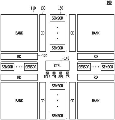
a control signal generation circuit having a plurality of signal shifting stages connected in series, the control signal generation circuit configured a) to sequentially shift a single test mode signal in response to a toggling of a clock signal, and b) to sequentially generate a plurality of control signals for controlling a plurality of temperature sensing circuits, using at least one sequentially shifted test mode signal obtained from a preceding stage of the plurality of signal shifting stages; and
the plurality of temperature sensing circuits each including a first resistor having a resistance that varies depending on temperature and configured to receive the plurality of control signals and generate a temperature sensing signal based on the resistance in response to a corresponding control signal of the plurality of control signals.
|