US 11,859,275 B2
Techniques to improve adhesion and defects for tungsten carbide film
Vivek Bharat Shah, Sunnyvale, CA (US); Anup Kumar Singh, Santa Clara, CA (US); Bhaskar Kumar, Santa Clara, CA (US); and Ganesh Balasubramanian, Fremont, CA (US)
Assigned to Applied Materials, Inc., Santa Clara, CA (US)
Appl. No. 16/960,277
Filed by Applied Materials, Inc., Santa Clara, CA (US)
PCT Filed Jan. 3, 2019, PCT No. PCT/US2019/012143
§ 371(c)(1), (2) Date Jul. 6, 2020,
PCT Pub. No. WO2019/139809, PCT Pub. Date Jul. 18, 2019.
Claims priority of provisional application 62/617,376, filed on Jan. 15, 2018.
Prior Publication US 2021/0108309 A1, Apr. 15, 2021
Int. Cl. C23C 16/02 (2006.01); C23C 16/32 (2006.01); C23C 16/455 (2006.01); C23C 16/513 (2006.01); C23C 16/52 (2006.01)
CPC C23C 16/0272 (2013.01) [C23C 16/32 (2013.01); C23C 16/45557 (2013.01); C23C 16/513 (2013.01); C23C 16/52 (2013.01)] 20 Claims
OG exemplary drawing
 
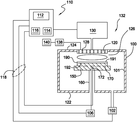
1. A method of forming a tungsten carbide film, comprising:
forming, by plasma-enhanced chemical vapor deposition (PECVD), a tungsten carbide initiation layer directly on a silicon-containing surface of a substrate at a first deposition rate; and
forming a tungsten carbide film on the tungsten carbide initiation layer at a second deposition rate, wherein the second deposition rate is greater than the first deposition rate.