| CPC B29C 70/683 (2013.01) [H01B 13/0036 (2013.01); B29K 2063/00 (2013.01); B29L 2031/34 (2013.01)] | 4 Claims |

|
1. A method of manufacturing an electronic device in which at least one electronic component coupled to a lead is covered with a mold cover, the method of manufacturing an electronic device comprising:
a coupling step of coupling a first electronic component to a first lead;
a bending step of bending the first lead to adjust a posture of the first electronic component; and
following the bending step, a molding step of molding the first electronic component with a resin material to form the mold cover, wherein
the bending step preventing return deformation of the first lead, the bending step comprises:
a first step of bending the first lead to a first angle of not more than 30 degrees, the first angle being less than a target angle by pressing a first pressing member against the first electronic component to move the first electronic component toward a mounting table supporting a lead frame of the electronic device during manufacture;
a second step of bending the first lead to a second angle of not less than 30 degrees and not more than 60 degrees, the second angle being less than the target angle by pressing a second pressing member against the first electronic component to move the first electronic component toward the mounting table supporting the lead frame of the electronic device during manufacture; and
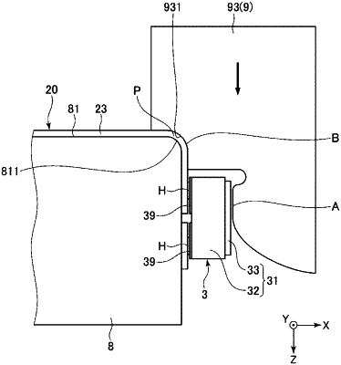
a third step of bending the first lead to the target angle by pressing a third pressing member against the first lead in a first direction without pressing the third pressing member against the first electronic component to move the first electronic component toward the mounting table supporting the lead frame of the electronic device during manufacture, a portion of the third pressing member overlaps the first electronic component in a second direction tangential to the first direction without contacting the first electronic component.
|